
Toyota 4Runner: Data Signal Circuit between Radio Receiver and Stereo Jack Adapter
DESCRIPTION
The No. 1 stereo jack adapter assembly sends the sound data signal or image data signal from a USB device to the radio and display receiver assembly via this circuit.
WIRING DIAGRAM
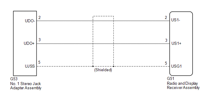
PROCEDURE
|
1. |
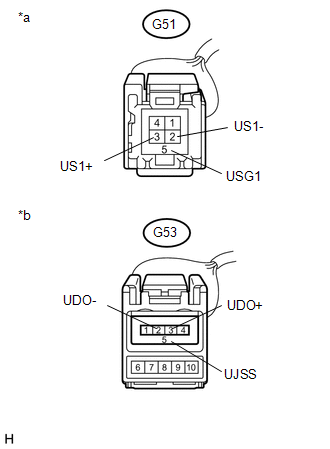
CHECK HARNESS AND CONNECTOR (RADIO AND DISPLAY RECEIVER ASSEMBLY - NO. 1 STEREO JACK ADAPTER ASSEMBLY) |
(a) Disconnect the G51 radio and display receiver assembly connector.
(b) Disconnect the G53 No. 1 stereo jack adapter assembly connector.
|
(c) Measure the resistance according to the value(s) in the table below. Standard Resistance:
|
|
| OK | .gif) |
PROCEED TO NEXT SUSPECTED AREA SHOWN IN PROBLEM SYMPTOMS TABLE |
| NG | |
REPAIR OR REPLACE HARNESS OR CONNECTOR |
 Sound Signal Circuit between Radio Receiver and Stereo Jack Adapter
DESCRIPTION
The No. 1 stereo jack adapter assembly sends the sound signal from an external
device to the radio and display receiver assembly via this circuit.
The sound signal that has been sent i ...
 Data Signal Circuit between Radio Receiver and Extension Module
DESCRIPTION
The stereo component tuner assembly sends the sound data signal or image data
signal from a device to the radio and display receiver assembly via this circuit.
WIRING DIAGRAM
PROCED ...
Other materials about Toyota 4Runner:
Installation
INSTALLATION
CAUTION / NOTICE / HINT
PROCEDURE
1. TEMPORARILY INSTALL BRAKE MASTER CYLINDER PUSH ROD CLEVIS
(a) Install the lock nut and brake master cylinder push rod clevis to the brake
booster assembly.
HINT:
Tighten the lock nut after adjusting the ...
Floor mat
Use only floor mats designed specifically for vehicles of the same model
and model year as your vehicle. Fix them securely in place onto the carpet.
Insert the retaining hooks (clips) into the floor mat eyelets.
Turn the upper knob of each retaining ho ...

0.0077